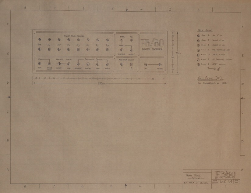
This is a simple 8 bit computer I designed in 1980, purely as a concept, inspired by the architecture of typical mini-computers of the 1970’s that I was trained and working on at the time. It was designed using standard TTL logic and would use micro-coding for the instruction fetch and execution, and all the front panel operations.
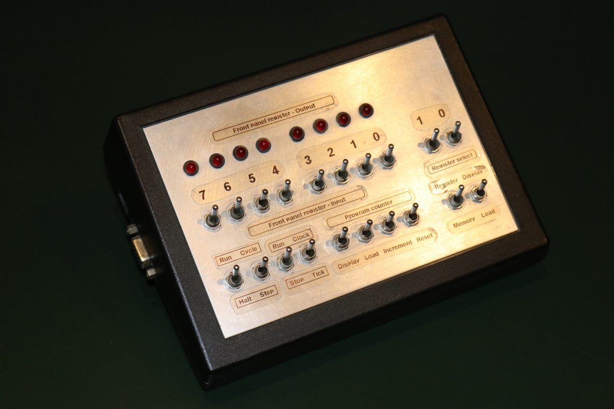
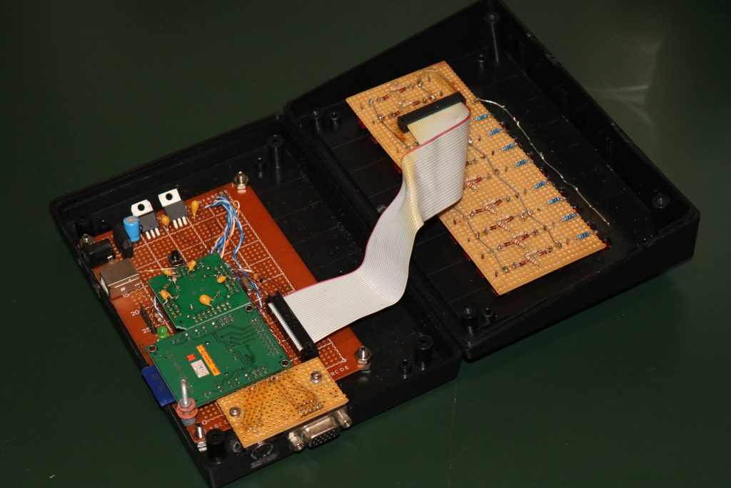
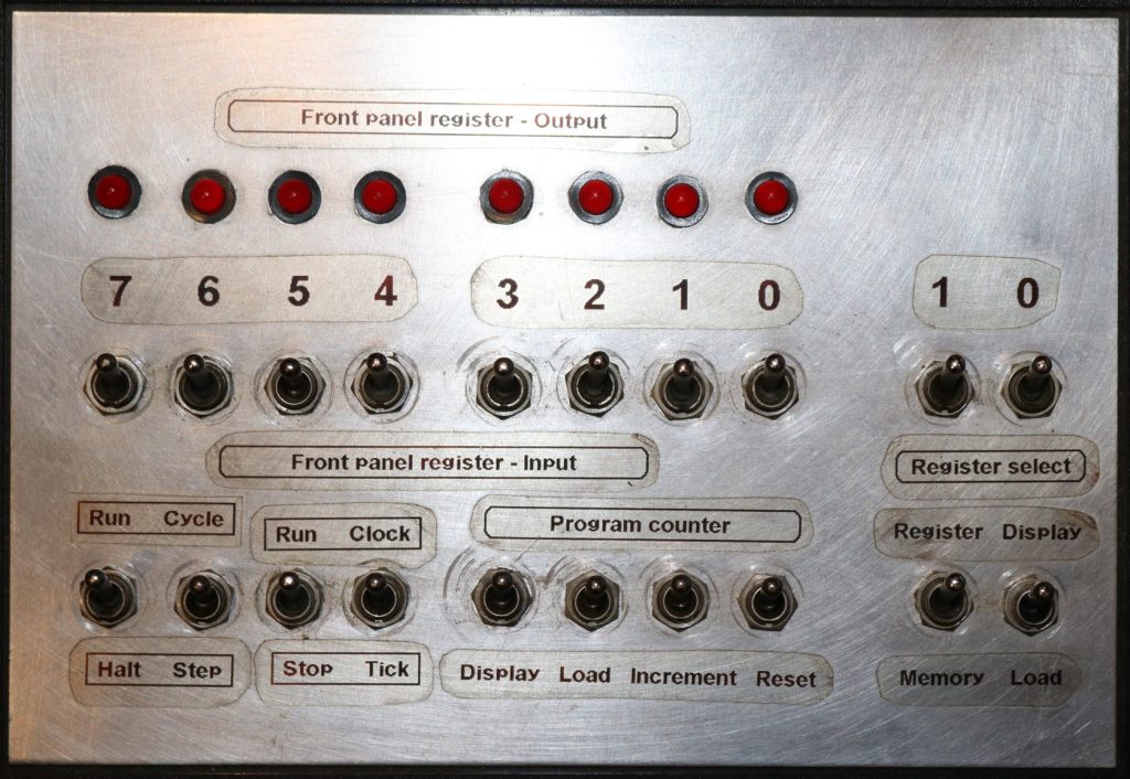
The only model I have built is shown above and below, but this is a cheat, because that is actually a Maximite computer with lights and switches attached to its GPIO, with the PB/80 emulated in BASIC code. But its entire operation is driven by the exact same micro-code as the original design, so it proves the concept.
This is a technical description of the operation and design of the computer, along with copies of some of my original (hand-drawn) circuit designs and documentation. This was never intended as a useful computer. It was simply an intellectual exercise to reinforce my training and knowledge at the time. And this is just an opportunity to bring all that documentaion together in one place.
Specifications
These are the key details of the design. A more detailed description is available in the scans of original documents above.
- 8 bit word size
- 256 byte memory
- 4 general purpose registers
- Arithmetic logic unit providing 16 operations including shift/rotate
- Up to 60 instructions
- Register, indirect, absolute and indexed addressing
- Micro-coded instruction control
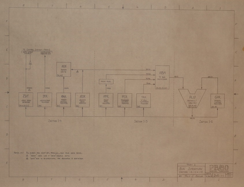
Bus structure
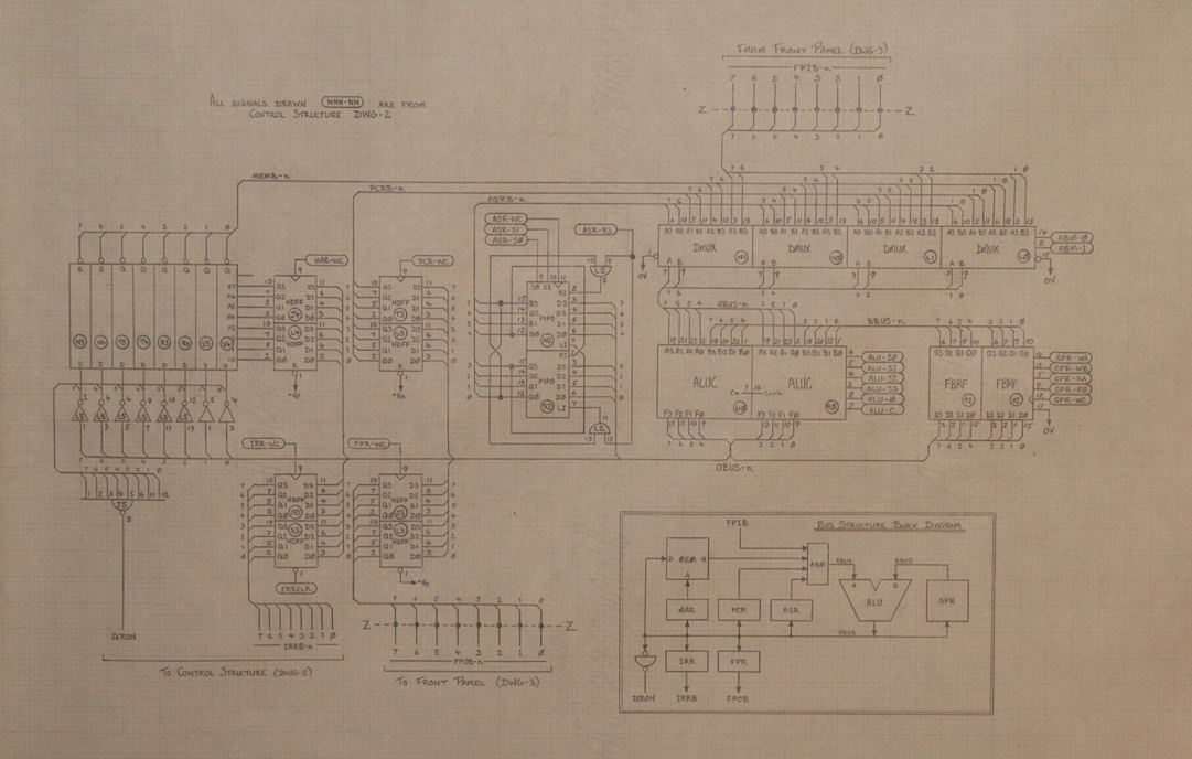
The structure of the computer is simple with an 8 bit bus at the A and B inputs of the ALU, and an 8 bit bus at its output. The B bus selects from one of four general purpose registers, and the A bus selects from the program counter (PCR), memory (MEM), front panel switches (FPR) or a temporary register (TRA). The output from the ALU can write to 7 destinations including all off the above, plus a memort address register (MAR) and the instruction register (IRR).
This structure has been very consistent right from the original design which you can find here. These design articles are quaint and hilarious at the same time. They even include anotations by my bored girlfriend at the time. But I cannot have been totally boring; we have been married now for 40 years.
Micro-code instructions
All operations in the computer architecture are controlled by “micro-codes” contained in a ROM consisting of 256 words of 12 bits each. The 12 bits are divided into 5 fields which select the source, destination and operation of elements in the bus structure and results of the instruction execution. The 5 fields and there purpose are;
- RCA – 2 bits – ALU “A” bus source
- RCB – 1 bits – ALU “B” bus source (register zero or register ‘n’)
- RCC – 4 bits – ALU operation (16 possible operations)
- RCD – 3 bits – ALU result destination
- RCE – 2 bits – Instruction execution “end” control
The complete ROM code of the original design can be found here. The 5 fields and their opcodes have not changed throughout the various iteration of the design. But front panel operations, which are encoded on pages 15 and 16 are different in the final design.
Instruction execution cycle
An instruction has the opcode in the top 6 bits of the byte and a register address in the lower 2 bits. Absolute and relative memory addresses or other operand may be be supplied in the next byte.
  7   6   5   4   3   2   1   0
+---+---+---+---+---+---+---+---+
|          opcode       |  reg  |
+---+---+---+---+---+---+---+---+
|  optional operand or address  |
+---+---+---+---+---+---+---+---+
The opcode will be used directly as the address of the micro-code ROM, with the lower 2 bits substituted to contain a counter for the instruction execution cycles (T0 thru T3). So an instruction with an opcode, such as 8A (100011RR) will address micro-code ROM locations 8A thru 8F for execution cycles T0 thru T3.
The execution cycle is incremented until the RCE bits of the micro-code and the result from the ALU match one of four conditions;
- RCE = 0 – Continue (Unconditional continue)
- RCE = 1 – End if not zero
- REC = 2 – End if zero
- RCE = 3 – Unconditional end
So for example, a conditional instruction, such as JNZA (jump not zero absolute) has an opcode of A0 and three execution cycles (T0 thru T2). These combine to address ROM locations A0, A1 and A2, and the micro-code definition for this instruction is defined as;
- T0 – Read program counter (PCR) from A bus, increment A bus and write to PCR and memory address register (MAR)
- T1 – Read register ‘N’ (addressed by lower 2 bits in the instruction byte) from B bus, and write it to temporary register A (TRA). If the output of the ALU is zero the RCE field indicates that the instruction will end.
- T2 – Otherwise, read contents of memory addressed by MAR (loaded in cycle T0) from A bus, decrement A bus and write it to the program counter and memory address register. The RCE field indicates that the instruction will end unconditionally.
The effect of all of this is that if the contents of the general purpose register (addressed by lower 2 bits in the instruction byte) is not zero, the next instruction will be fetched from the absolute address contained in the second byte of the instruction. Note that this value is decremented in cycle T2 before it is written to the program counter, because the program counter will be incremented in the next instruction fetch cycle.
Additionally, the instruction cycle will not increment past T3. This is used by the DLY (delay, see above) instruction which will decrement the value of the operand until it reaches zero, so the last cycle contains an RCE code of 2, so the instruction will repeat cycle T3 until the operand is zero.
Instruction fetch cycle
The next instruction is retrieved from memory before each instruction execution cyle by two fetch cycles F0 and F1. These are located at ROM addresses locations FE and FF. Here is the ROM coding for these two locations;
- F0 – Read program counter (PCR) from A bus, increment A bus and write to PCR and memory address register (MAR)
- F1 – Read contents of memory addressed by MAR from A bus and write it to the instruction register (IRR).
Front panel micro-code cycles
When the computer is halted, it will execute micro-code at ROM addresses locations F0 thru FE (even addresses only). These addresses are determined by the position or action of the front panel switches, and the register selected by the display and load operations is determined by the register switches on the front panel;
- location F0 – Display register
- location F2 – Display memory
- location F4 – Load register
- location F6 – Load memory
- location F8 – Load program counter (PCR and MAR)
- location FA – Display program counter
- location FC – Reset program counter (PCR and MAR)
- location FE – Increment program counter (PCR and MAR)
Note that the “increment program counter” micro-code (location FE) is the same as that used for the first instruction fetch cycle (cycle F0). When the computer is running and the “reset PCR” switch is toggeled on the front panel, ROM location FC will be executed for cycle F0 instead. i.e.; toggling the “reset PCR” switch while the computer is running will reset the program counter to zero.
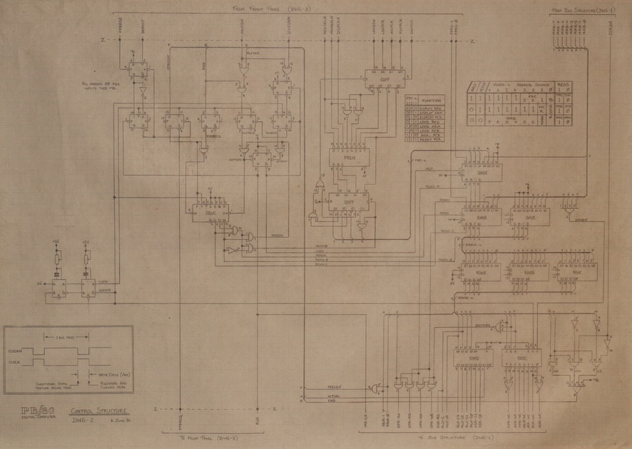
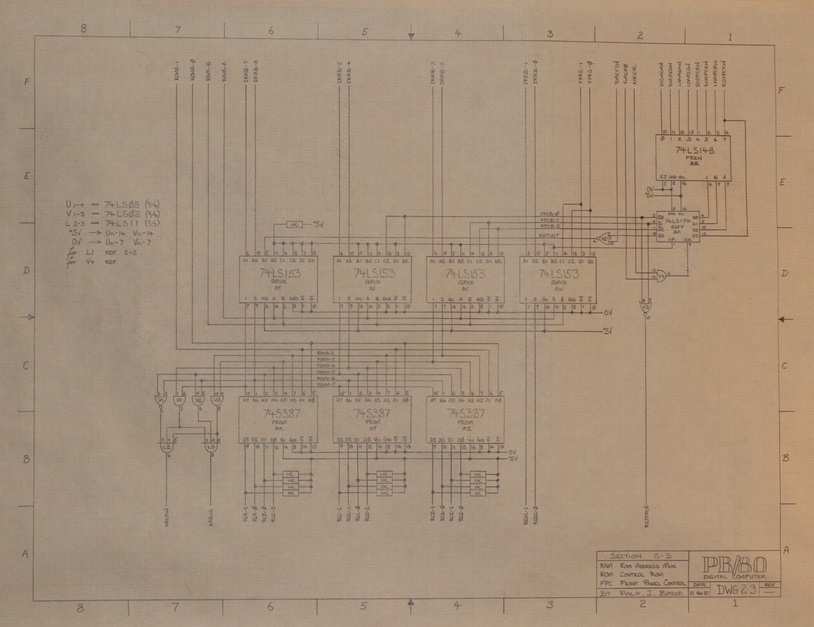
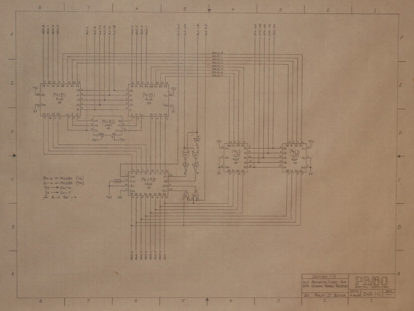
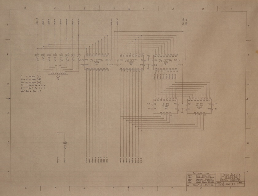
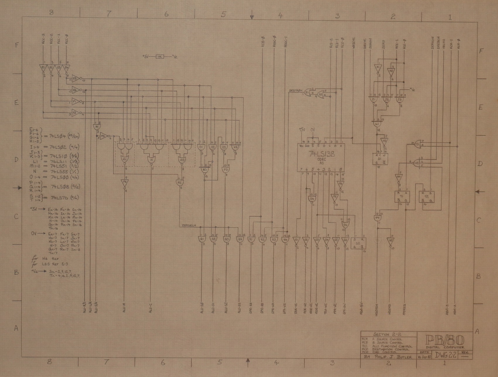
Circuit design
A later and more detailed circuit design was hand drawn on A2 sheets. This is the initial design;
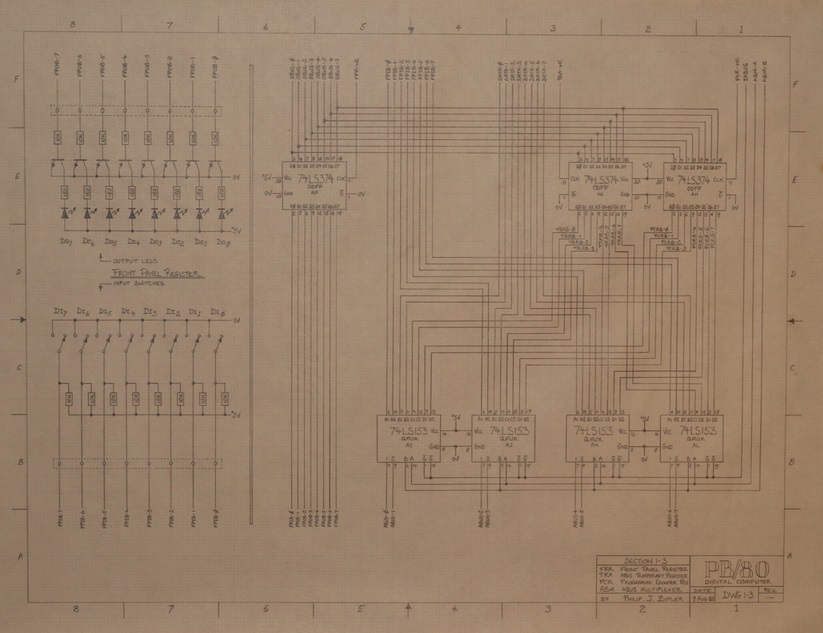
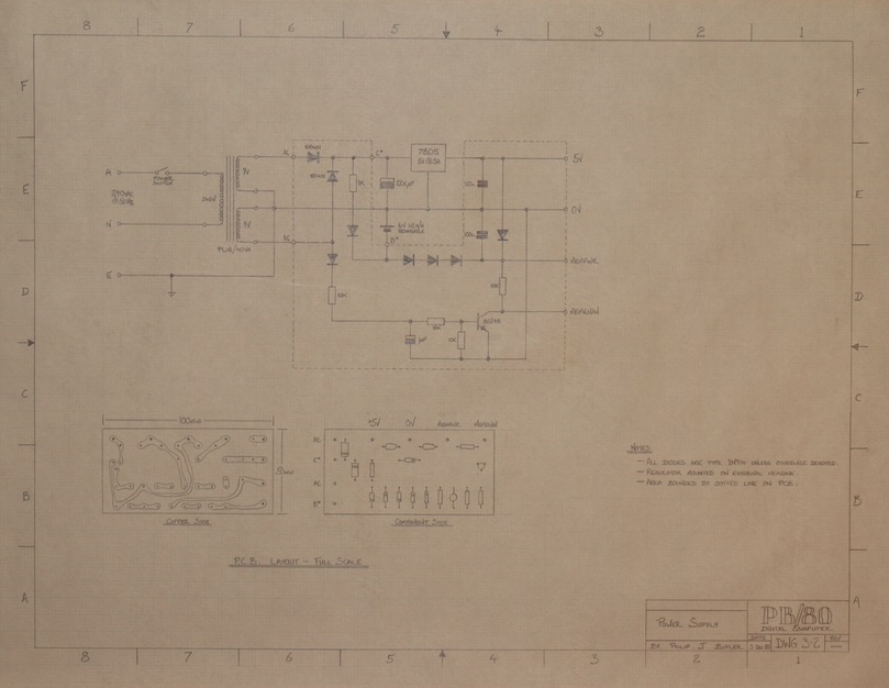
The circuit went through several versions. Here is a more recent version with simplified layout on two sheets;